Introduction
This article is background reading for Burning a 16 bit EPROM with an 8 bit programmer. It is heavy on detail and not really necessary other than for interest (that's why it's not in the main article).
What is a ROM and why do we care?
A ROM (Read Only Memory) is a type of computer memory that retains its data even when there is no power, but cannot be written to by the consumer (i.e. it is read only). Factory programmed mask ROMs were often used in older computers to store programs including the operating system, such as the Amiga Kickstart or game cartridges. An EPROM is simply a ROM that can be programmed and erased by the consumer using a special programmer and UV eraser. Old software can often be obtained as an image of the ROM they were released on, and customised images such as the custom Amiga Kickstart ROMs can be created, making the ability to program EPROMs extremely useful for people who still use and maintain old systems.
Memory organisation
Buses, bits, nibbles, and bytes
A line is a line on a circuit diagram that corresponds with a trace on the PCB. For the purposes of this document, a bus is a group of lines connecting two or more devices inside the computer. We are interested in two buses - the data bus, which moves data between devices inside the computer (such as between the CPU and memory), and the address bus, which the CPU (and some other devices like the Amiga custom chips) use to select which device is talking to the data bus.
The basic unit of computer memory is the bit. It is represented in the physical electronics as a data line that can either be low (0 v) or high (5 volt in older machines) and is represented in software as a binary number with the value of either 0 (low) or 1 (high).
A group of 4 bits is called a nibble, and represented in the circuit by a four bit wide data bus (i.e. four data lines). A nibble could be represented in software in binary, e.g. 15=1111b, 10=1010b etc. or it could be represented in hexadecimel (hex), using the numerals 0-9 and the letters a-f to represent the 16 possible combinations (15=1111b=Fh; 10=1010b=Ah). Note that the lowest value of a nibble is 0 (binary 0000b) not 1 and the maximum value is 15 (1111b).
The next unit is the byte, being 8 bits or two nibbles. It is represented in electronics as an 8 bit wide data bus. A byte can be any of 256 possible values, and is usually represented in programming as a two digit hexadecimel (i.e. 164=A4h=10100100b). A single byte also represents an ASCII character. As with nibbles, the lowest value of a byte is 0 (00000000b or 00h) and the highest value is 255 (11111111b or FFh).
Memory organisation and addressing
A computer's memory is organised in bytes (bytewise) in a memory map, and each byte has an address, a location in the memory. The size of the system's memory map is determined by the size of the CPU's address bus.
When the CPU needs to access memory it puts the address on the address bus and will set control bit as either low or high bit tell the system whether it is reading or writing.
Each address points to a byte of data. The Amiga's Motorola 68000 CPU has a 24 bit address space*, meaning that there are 2^24=16,777,216 (16M) addresses, and the CPU can address 16 mb of memory (full 68020s and above have 32 bit addressing). Addresses are represented using hexadecimal, with 000000h being the lowest address and FFFFFFh being the highest.
*Note for pedants. The M68000 actually only has 23 address lines; there is no A0 pin so it can only address even-numbered addresses. That is not a problem because the data bus is 16 bits (2 bytes) wide. The CPU can address 16 mb of memory but must do so by reading two bytes at the same time.
Words and endianness
The final unit we are interested in is the word. The length of a word depends on the data bus width of the system - for 16 bit systems such as those using the M68000 a word is always 16 bits or two bytes wide and there are 65536 possible values. The word is represented by two bytes, generally as hexidecimal (e.g. 23,456=5B A0h) but can also be read as ASCII code (47 4Ch="GL").
Most CPUs can only address a word of data rather than a particular byte. This means that a 16 bit CPU can only address every second byte, or even numbered addresses (as noted above the M68000 doesn't have an A0 line on its address bus). The odd-numbered addresses are read as an offset to the even numbered byte, so reading address EA0000H will return the byte at address EA0000H and EA0001H (since the CPU always reads an entire word at once). There is no particular scientific or engineering reason behind which order the two bytes of a word are put into memory; rather it is determined by convention and decided by the designers of a particular CPU.
The 16 bit Motorola 68000 CPU puts the most-significant byte (the byte with the most-significant bit, otherwise known as the "Hi Byte") into memory at the base address (the address actually on the CPU's address bus) and the least-significant byte ("Lo Byte") is put at the offset address (the next address in the memory map). The most-significant byte is always at an even address and the least-significant byte is always at an odd address. Consider the number 23,456=5BA0h being put into address EA0000H. The byte 5Bh would be put into address EA0000 and the byte A0h would be put into address EA0001H. This is called big-endian or the Motorola Convention and has the advantage that the word can be read in order from left to right when the addresses are increasing from left to right.
By contrast, the 16 bit Intel 8086/80286 CPUs put the least-significant byte into the byte at the base address and the most-significant byte at the offset address. The least-significant byte is even and the most-significant byte is odd. Using the example from the previous paragraph, the byte A0h would be put into address EA0000H and the byte 5Bh would be put into address EA0001H. This is called little-endian or the Intel Convention and has the advantage that files stored byte-wise (such as ROM images) are addressed in order - byte 0 is at address 0, byte 1 is at address 1, and so on.
The endianness means that the bytes in ROM images are not in the correct order for the big-endian M68000 (and believe that this is the same for Sega Megadrive and Atari ST ROMs). It is easy to fix by a process called byte swapping and is discussed on the project page of these instructions.
ROMs
ROMs are simply memory and are addressed exactly the same way as above. 16 bit Amiga Kickstarts above v 2.0 use the 256 kbit (kilobit) * 16 bit = 4 Mbit MX23C4100 mask ROM, with an 18 bit address bus. It can hold 2^18=262,144 addresses * 16 bit = 512 kB of program (versions 1.2 and 1.3 use a 128 kbit / 256 kB ROM). The 18 address lines are connected to the 18 least-significant CPU address lines
(i.e. A1-A18). The remaining CPU address lines are connected to glue logic (custom logic circuitry; except for the A1000 this is in Gary, Gayle, or Akiko) which decodes the address from the CPU. When the CPU asks for an address in the ROM the glue logic will send a low signal to the gate/output enable pin on the ROM, telling the ROM to output its data. When the CPU wants to read from a ROM at a particular address it will output the address for the on the address bus then read back a 16 bit word from the data bus:

It is electrically equivalent to put two 8-bit ROMs on the bus. Both ROMs share the Address Bus, while the data lines for one ROM will connect to the data lines for the even byte and the other for the odd (offset) byte:

It is noteworthy that Commodore did the same thing in the 32 bit Amigas (A1200, A3000 and A4000), but using two 16 bit ROMs on the high and low halves of the 32 bit data bus.
If we have a CPU with an 8 bit data bus and access a 16 bit ROM the CPU will only read the most-significant byte (even byte) and the odd byte is ignored (since it is disconnected from the bus). Many or most 16 bit ROMs may also be wired up in 8 bit mode.

Connection details
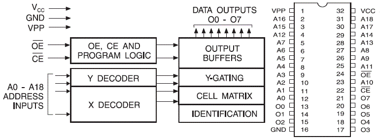
A ROM has four types of pins: power supply, program logic, address bus, and data bus. The power supply supplies power for the IC to operate and for 1980s computers it usually consists of a VCC pin at 5 v and a GND (0 v), although this can vary. EPROMs also require a programming voltage (discussed in the project section). The address bus tells the ROM which data to look at, with the number of address lines is determined by the size of the ROM. The data bus is where the ROM outputs the data; in our case there are 16 of them: D0-D15, with D0-D7 being the even byte and D8-D15 the offset byte. The program logic usually consists of two pins, Chip Enable (/CE) and Output Enable (/OE, sometimes called the Gate /G). The /CE pin must be low to bring the chip online, and the /OE pin must be low to output on the data bus. While the /CE and /OE both have the same function (to enable or disable output from the ROM) the /OE pin is much faster as it controls logic gates at the output. The logic diagram and pinout for the 27C040, an 8-bit EPROM, is shown below:

EPROMs
When software is released from the factory it is usually released on a mask ROM, a ROM that is programmed in the factory using the photolithographic method. The description of how this is done is outside the scope of this document but is interesting nonetheless. Consumers have the option to program many types of non-volatile memory, of which the EPROM is just one type.
How EPROMs work
EPROMs are an array of floating gate transistors, and an description of the physics of how they work is unfortunately outside the scope of this document. It can be visualised as an array of fuses representing each data bit. When an address is put on the ROM's address bus (and the CE and OE lines are low) the value of the fuses at that address is output on the data lines. When the EPROM is shipped the fuses are all intact (output high); if the computer addresses the EPROM it will output all data lines high at every address (i.e. every single byte is FFh). When the EPROM is programmed the programmer blows some of the fuses so that when the EPROM is addressed after programming it will return the programmed data, just like a mask ROM. The fuses can be reset to factory (all bytes FFh) by exposing the EPROM's window to a particular wavelength of UV light (253.7 nm) for a particular amount of time (about 20 minutes).
EPROMs for the Amiga
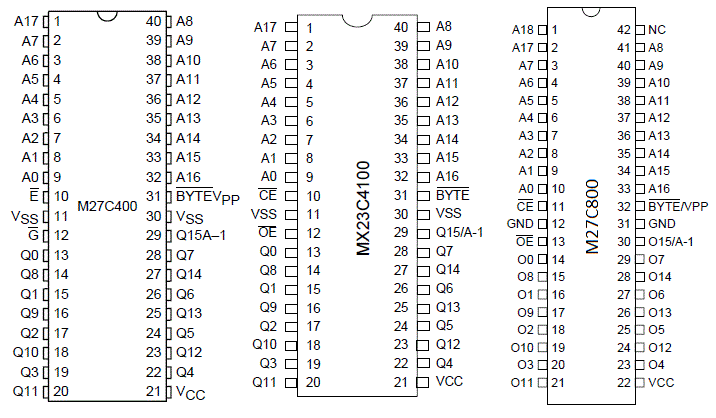
As mentioned above, 16 bit Amiga Kickstart ROMs above v 2.0 were released on the MX23C4100 4 Mbit (512 kB) mask ROM. This mask ROM is pin-compatible with an EPROM, the 27C400:

Kickstart 1.2 and 1.3 can also be used with this EPROM, all that is required is to program two images back to back by concatenating the ROM image onto itself before burning.
The 27C800 is the 8 Mbit brother of the 27C400 and is pin-compatible except for having two extra pins (one extra address line and one that is not connected). It is possible to program two ROM images (e.g. Kickstarts 1.3 and 3.1), each taking half the EPROM, and select them using a switch connected to pin A18:

Programming EPROMs
Programming EPROMs involves putting a much higher than usual voltage across some of the bits in order for them to return LOW. To do this the programmer increases VCC to 6.25 v and puts a programming voltage, VPP, of between 12 and 13.5 v on pin /BYTE/Vpp. With the two control lines (/OE & /CE) high, an address is put on the address bus and the data for that address is put on the data bus. After a 2 us delay for voltages to stabilise the /CE (or /E) pin is pulsed low for 50 us and the data is saved at that address. After /CE is brought high again the programmer will wait 2 us, remove the data from the data bus, wait another 2 us, pulse /OE (or /G) low and read the data back to verify it.
Most programmers will read the entire EPROM normally to make sure it is blank, write the data using the above sequence, then verify the entire EPROM by reading it back normally.

Programming a 16 bit ROM with an 8 bit programmer
The 27C400 and 27C800 are signal-compatible with the 27C040, a 512k * 8 bit = 2 Mbit or 512 kB EPROM, with the only difference being that there are only 8 data lines instead of 16. This means that with a suitable adapter we can trick the programmer into programming each byte in the word separately. All we have to do is split the ROM image into images for the high and low bytes, and program each byte separately.
There are two traps. First it must be ensured that the data lines for the byte not currently being programmed cannot accidentally have a low signal. This is easily achieved by connecting them to the VCC rail via pull-up resistors (any value between 4k7 and 47k will work).
Second is that the 27C400 has one fewer address line than the 27C400: the 27C040 needs 19 address lines to access its 512 kB of data because its data bus is half the size of the 27C400 (the 27C040 can be considered to be half of a 27C800) and the programmer will not program because it detects a pin is not connected. While there is a 27C020 that could be considered half of a 27C400, it is not signal compatible during programming since there is a separate program strobe pin - this function is achieved with the CE pin on the 27C040 and the two 16 bit EPROMs we are interested in. We can solve this problem by tricking the programmer again, this time by connecting a resistor between pin 1 (A18) and GND, making it appear to the programmer that the pin is connected. It will program the EPROM twice, so we have to make sure the second half of the ROM image to be programmed is high (FF). Note that the verification step will fail at exactly half way :-).
 Total Members: 180
 Latest: chrise
 Total Posts: 1983
 Total Topics: 479
 Online Today: 77
 Online Ever: 262
 Users: 0
 Guests: 28
 Total: 28

Vampirella of Drakulon by intangybles
April 2025 - Project X Sp... by NinjaKat
March 2025 - Belial by NinjaKat
Amiga Retro Brisbane V4SA... by intangybles
 AMIGA/040 - Amiga 40th An...
by Marcio D.
 February 2025 - Cave Runn... by NinjaKat
AmiExpress (/X) BBS Runni... by intangybles
Welcome to the new BBS In... by intangybles
Amiga Retro Brisbane BBS ... by intangybles
 3D Library for PiStorm-eq...
by Marcio D.


